UTAustinX: UT.6.x Embedded Systems Shape the World
Index
C1 Introduction
- A system is comprised of components and interfaces connected together for a common purpose
- An embedded system its a system that (optionally) combines multiple types of components for example mechanical, electrical, and chemical component along with a computer or a processor unit to perform a single dedicated purpose.
C2 Fundamental Concepts
Considerations of Good Embedded Systems
- Testable to verify and guarantee functionality
- Power efficient because usually run on batteries
- Size fit it an specific size
- Time Not only getting the correct answer but getting it at the right time
- Profitable. Profit is a combination of market share and cost
- market share - making something everyone wants to buy. The percentage of market share a company has on a certain market means the percentage of people that want to buy your product (and of course can buy it in that market)
- cost - how much resources it takes to make something
A real-time system it s system that can guarantee a worst case upper bound on the response time between when the new input information becomes available and when that information is processed.
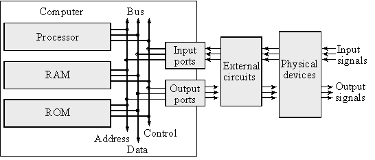
A computer combines a processor, memory (RAM: random access memory, ROM: read only memory), and input/output (I/O) ports and devices
- Von-Neuman Architecture: Same bus for data and code/instructions
- HarvardArchitecture: Different bus for data and code/instructions
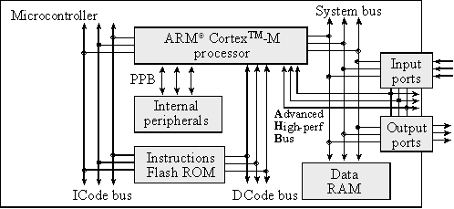
Cortex M4 Summary & Features
- Instructions are fetched using the ICode bus
- Some internal peripherals,communicate directly with the processor via the PPB (private peripheral bus); the NVIC (nested vectored interrupt controller) is an example of this
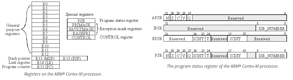
- Registers are high-speed storage inside the processor.Cortex M4 has 13 general purpose registers (R0-R12) for data manipulation operations and other special purpose registers (R13:SP, R14:LR, R15:PC, PSR...).
- The ARM Architecture Procedure Call Standard, AAPCS, part of the ARM Application Binary Interface (ABI), uses registers R0, R1, R2, and R3 to pass input parameters into a C function and place the return parameter in Register R0.
- Cortex M4 has 8 levels of interrupts priority, 0: highest priority ; 7: lowest priority, we use BASEPRI register to set this priority.
- to enable/disable/mask interrupts the registers PRIMASK (for most interrupts) and FAULTMASK (for all interrupts) are used (of course NMIs: Non-Maskable interrupts are not affected by these mask registers)
Assembly
- Cortex-M microcontrollers, executes Thumb instructions extended with Thumb-2 technology
- Cortex M4 Assembly Reference
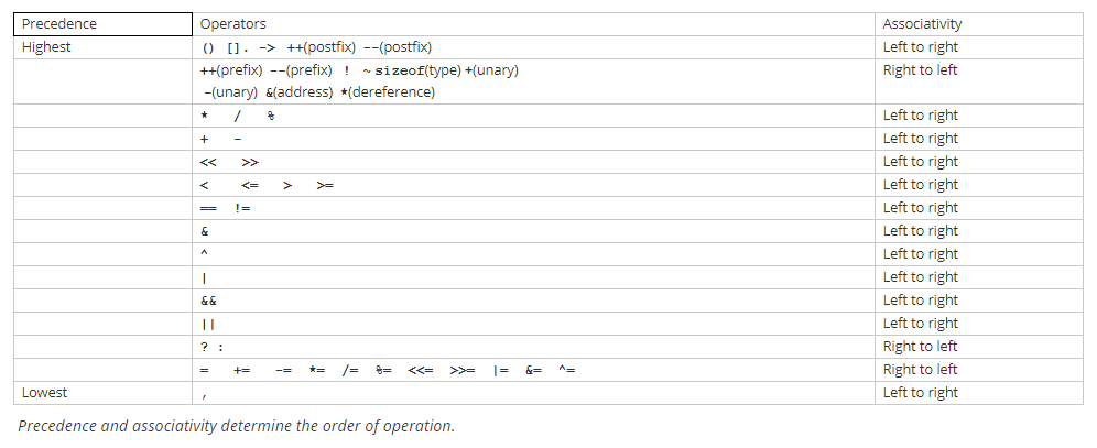
- In general in an instruction, data flows towards the op code (right to left)
- Assembly Language Instructions Fields:
- label: This field is optional and is used to identify the position in memory of the current instruction (must have unique name for each label).
- opcode: This field specifies the processor command to execute.
- The operand field specifies where to find the data to execute the instruction.
- Thumb instructions have 0, 1, 2, 3, or 4 operands, separated by commas.
- comment optional to add comments
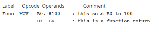
- Instructions categories:
- Memory Access E.g.
load, store
- Arithmetic/Logic Operations E.g.
ADD, SUB, AND, LSL, etc.
- Control Operations Change the flow of code, branch operations. E.g.
BEQ
- Special Instruction E.g. Instructions to turn on interrupts. E.g.
BEQ
When we build a project all files are assembled or compiled then linked together. The address values shown in the listing
are relative to the particular file being assembled. When the entire project is built, the files are linked together,
and the linker decides exactly where in memory everything will be. The assembler/compiler may also produce a listing file,
which is a human-readable output showing the addresses and object code that correspond to each line of the source program.
Addressing modes
- Addressing mode defines how the instruction will access the data it needs.
- If the data is found in the instruction itself, like
MOV R0,#1, the instruction uses Immediate addressing
- Indexed addressing mode uses a register pointer to access memory.
- The addressing mode that uses the PC as the pointer is called PC-relative addressing mode, it's used for branching, calling functions and access data in ROM, etc.
- The machine code contains the address difference between where the program is now (the program counter
PC) and the address to which the program will access.
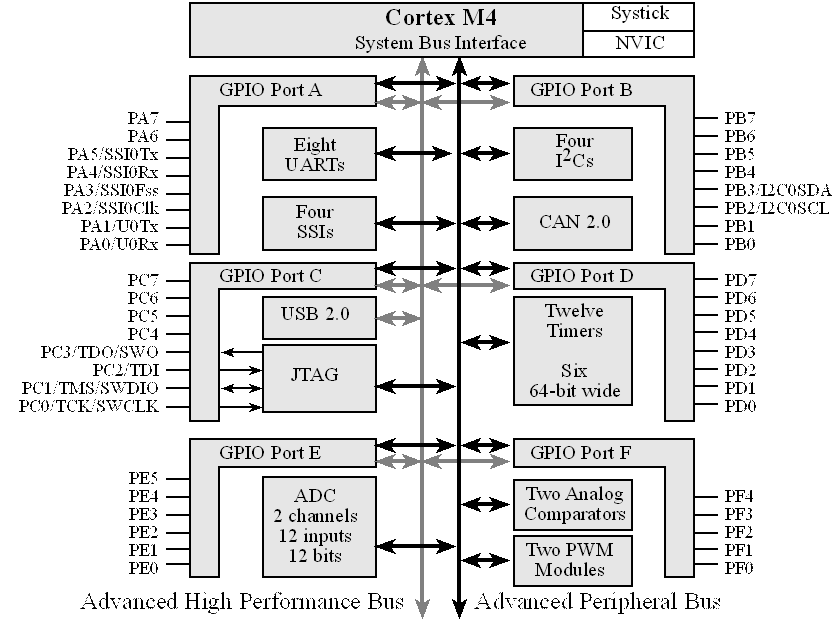
TM4C123
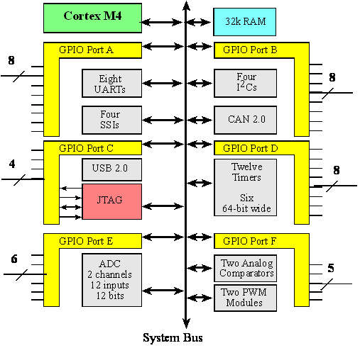
- TM4C123 is Harvard architecture microcontroller based on ARM Cortex M4
- It has 32kB of SRAM, 256kB of Flash
- Up to 43 GPIOs 5 ports (A, B, C, D, E, F)
- Provides an integrated ICDI (In-Circuit Debug Interface)
- PC3, PC2, PC1 and PC0 are reserved for debugger
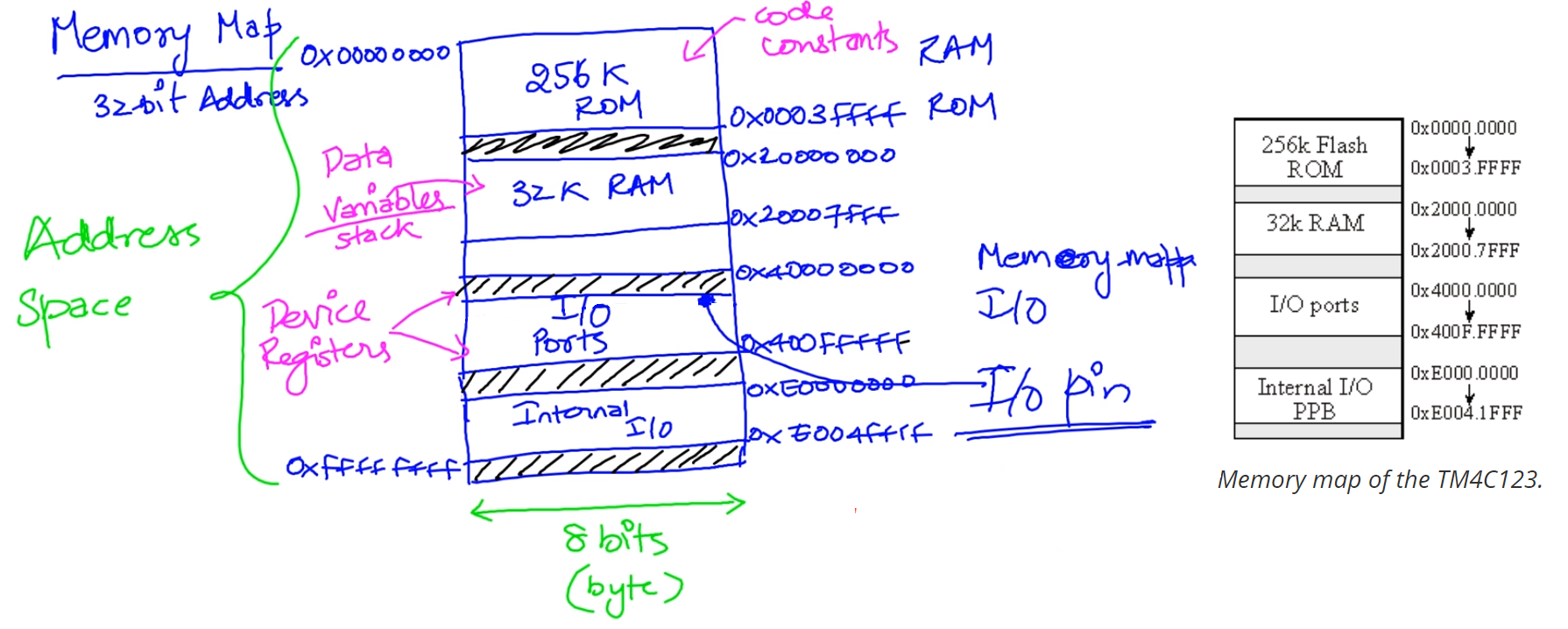
Memory Map / Memory Mapping
- Uses to abstract to the SW the fact that there can be multiple physical devices which are the ones that actually store the information
- SW thinks there is only a single memory so it only needs to worry about providing a single address
- Address space Total memory we can refer. It constitutes the number of locations we can refer to.
- With 32-bits we can refer from 0x0 to 0xFFFFFFFF
- We refer to I/O using a technique called memory-mapped I/O.
- The devices are mapped to a region of the memory map so the can be access through read/writes to memory
- When we want to refer to a device, we simply read or write a particular location in memory, and that particular location refers to an I/O device registers
ISA
- Set of Operations supported
- Data types (integer, floating point)
- Registers (general purpose, special registers)
- Addressing Mode (How data is formed)
- Memory Access
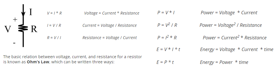
C3 Basic Electronics
Ohms law, voltage, resistance, current & power
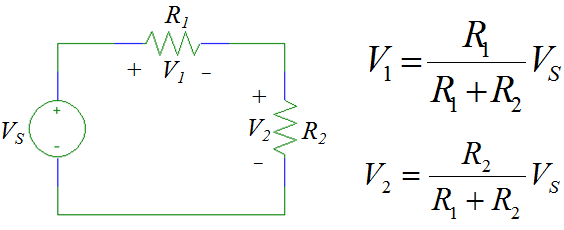
Voltage divider/division
C4 Digital logic
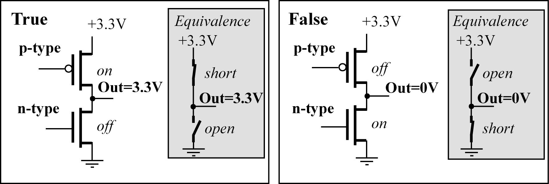
n-channel and p-channel transistors for digital logic
- The following image shows the output of a typical complementary metal oxide semiconductor (CMOS) circuit
which is a common basic building block used in many parts of digital systems and as the base of other more complex digital circuits
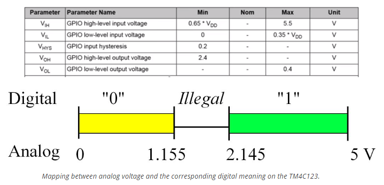
Logic high and low
- VOH & VOL output voltage for high and low states
- VIH & VIL input voltage for high and low states
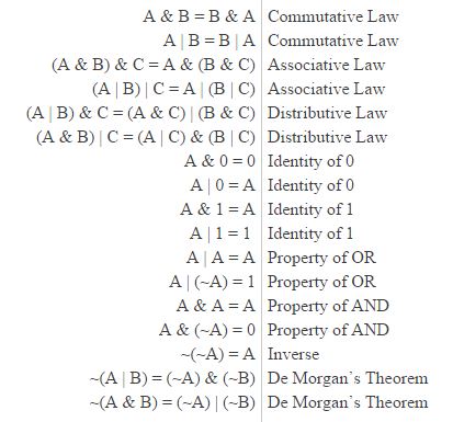
Boolean Algebra
Other digital blocks
- The outputs of a latch respond to the voltage levels of their input, whereas flip-flops are edge-triggered.
For a D flip-lop the output changes on the rising edge of the input clock.
- The tristate driver can be used dynamically control signals
- Has three possible outputs: high, low, and HiZ.
- When the driver is active, its output (Y) equals its input (A). When the driver is not active, its output Y floats independent of A
- The output of an open collector gate, the has two states low (0V) and HiZ (floating), we can use the open collector NOT gate to switch current on and off to a device,

- We can build an 8-bit storage element (memory), shown logically as by combining 8 flip-flops. This basic storage element is called a register
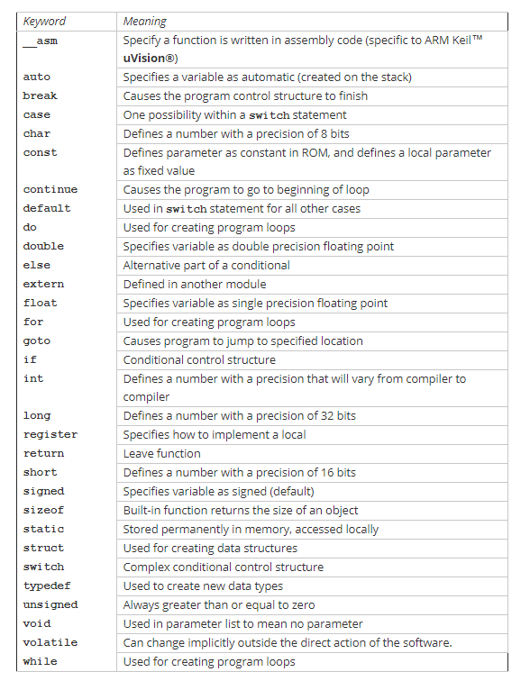
C5 Introduction to C
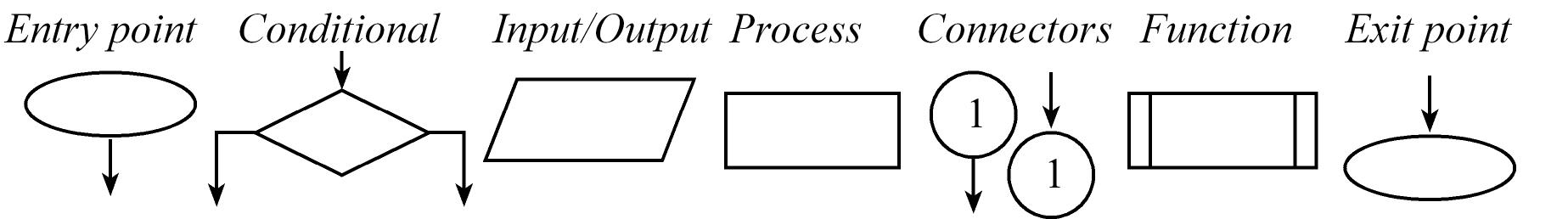
Flowcharts
- Describe the flow of a program, describes what are the paths a program can take
C Programming language
- Structured language, so supports the following templates: sequential, decision, iterative
- The C language is tightly coupled to the physical hardware of the machine (I/O) compared to other languages
- In 1999, the language C99 was developed. And this is actually a professional language that adheres to very strict standards but it's slightly different from pure original C
A very powerful approach to I/O is to provide a high-level abstraction in such a way that the I/O device itself is hidden from the user. printf is a clear examples of this in
which we can init an I/O (like a UART) for example and then implement fputc correctly so we can use printf to print/output data to the UART. printf reference
- The
volatile keyword disables compiler optimization, forcing the compiler to fetch a new value each time. We will use volatile
when defining I/O ports because the value of ports can change outside of software action. We will also use volatile when sharing
a global variable between the main program and an interrupt service routine.
C6 Microcontroller Ports
- General purpose (Parallel) I/O Ports or GPIO, allows us to exchange digital information with the external world
- It's one of the most basic input/output interfaces in embedded systems
- Pins on the LM4F/TM4C family can be assigned to as many as eight different I/O functions.
- There are two buses used for I/O. The digital I/O ports are connected to both the advanced peripheral bus and the advanced high-performance bus.
Port I/O:
- input port has the direction register bit at 0 (
DIR_R=0). On read the value on the pin is then mapped on to the bus to read it
- output port has the direction register bit at 1 (
DIR_R=1). Latch a value to a register and that register writes/outputs the value to the pin
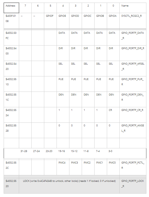
Pins PC3 – PC0 are reserved for the JTAG debugger
Each pin has one configuration bit in the GPIOAMSEL register to enable analog function (this means ADC or analog comparator) and in the GPIODEN to enable digital
Each pin has four bits (0 to 16 possibilities) in the GPIOPCTL register, which we set to specify the alternative function for that pin (0 means regular I/O port) and a GPIOAFSEL to enable the selected alternate function
GPIO Init/Config
- Enable/disable Digital functionality bits
GPIO_PORTX_DEN_R depending on what we want
- E.g.
GPIO_PORTE_DEN_R |= 0x00000003 // set bits PE 0,1 to enable digital functionality
- Enable/disable Analog functionality bits
GPIO_PORTX_AMSEL_R depending on what we want
- E.g.
GPIO_PORTX_AMSEL_R &= ~0x00000003 // clear bits PE 0,1 to disable analog functionality
- Select alternate functionality using corresponding field
PMCx in GPIO_PORTX_PCTL_R
- Each pin also has bits in the
GPIOPCTL register,
- E.g.
GPIO_PORTE_PCTL_R = (GPIO_PORTE_PCTL_R & 0xFFFFFF00) | 0x01 | 0x10; // set functionality to 1 on PE0-1 ; PE0<-PMC0=1 and PE1<-PMC1=1
- Enable/disable alternate functionality bits in
GPIO_PORTX_AFSEL_R depending on what we want
- E.g.
GPIO_PORTE_AFSEL_R |= 0x00000003 // set bits PE 0,1 to enable alternate functionality on those pins
All I/O devices also have a clock, we need to make sure to enable this clock in order to use certain I/O
- To initialize a GPIO as general I/O PORT, we perform 7 steps. Relevant Registers:
- `SYS_CTL_RCCN_R``: Clock enabler
GPIO_PORTX_LOCK_R & GPIO_PORTX_CR: Port unlocked and change enabler on port (Only some pins need this step to unlock)- Disable Analog functionality in
GPIO_PORTX_AMSEL_R
- Select PORT functionality in
GPIO_PORTX_PCTL_R
GPIO_PORTX_DIR_R: Direction 0: input ; 1: output- Make sure pins are configured as I/O ports
GPIO_PORTX_AFSEL_R (disable alternate functionality)
- Enable the pins in
GPIO_PORTX_DEN_R,
- For inputs we may also enable/disable pull-up resistors using
GPIO_PORTX_PUR_R bits -> 0: disable pull-up ; 1: enable pull-up
    #define GPIO_PORTF_DATA_R       (*((volatile unsigned long *)0x400253FC))
    #define GPIO_PORTF_DIR_R        (*((volatile unsigned long *)0x40025400))
    #define GPIO_PORTF_AFSEL_R      (*((volatile unsigned long *)0x40025420))
    #define GPIO_PORTF_PUR_R        (*((volatile unsigned long *)0x40025510))
    #define GPIO_PORTF_DEN_R        (*((volatile unsigned long *)0x4002551C))
    #define GPIO_PORTF_AMSEL_R      (*((volatile unsigned long *)0x40025528))
    #define GPIO_PORTF_PCTL_R       (*((volatile unsigned long *)0x4002552C))
    #define SYSCTL_RCGC2_R          (*((volatile unsigned long *)0x400FE108))
    #define GPIO_PORTF_LOCK_R       (*((volatile unsigned long *)0x40025520))
    #define GPIO_PORTF_CR_R         (*((volatile unsigned long *)0x40025524))
    #define SYSCTL_RCGC2_GPIOF      0x00000020  // port F Clock Gating Control

    ...

    void PortF_Init(void) {
      volatile unsigned long delay;

      SYSCTL_RCGC2_R |= 0x00000020;     // 1) activate clock for Port F
      delay = SYSCTL_RCGC2_R;           // allow time for clock to start

      GPIO_PORTF_LOCK_R = 0x4C4F434B;   // 2) unlock GPIO Port F
      GPIO_PORTF_CR_R |= 0x1E;          // allow changes to PF4-1, only PF0 needs to be unlocked, other bits can't be locked

      GPIO_PORTF_AMSEL_R &= ~0x1E;      // 3) disable analog on PF4-0

      GPIO_PORTF_PCTL_R &= ~0x000FFFF0; // 4) PCTL GPIO on PF4-0, select PORT functionality

      GPIO_PORTF_DIR_R &= ~0x10;        // 5) PF4 in (write 0 to this bit),
      GPIO_PORTF_DIR_R |= 0x0E;         //    PF3-1 out (write 1 to these bits)

      GPIO_PORTF_AFSEL_R &= ~0x1E;      // 6) disable alt funct on PF4-0

      GPIO_PORTF_PUR_R |= 0x10;         // enable pull-up on PF4 (only for inputs if needed)

      GPIO_PORTF_DEN_R |= 0x1E;         // 7) enable digital I/O on PF4-0
    }
Even though I/O operations "look" like reads and writes to memory variables, the I/O ports often DO NOT act like memory.
For example, some bits are read-only, some are write-only, some can only be cleared, others can only be set, and some bits cannot be modified.
C7 Design and Development Processes
Development process
- Requirements: Document what the system will do and what we need to do it
- Design: Algorithms, Diagrams, flowcharts...
- Testing Design: Simulation
- Development: Actual creation of HW and SW
- Testing: testing of the actual system
- Deployment: release
A requirement is a specific parameter that the system must satisfy. A requirement is usually defined in general terms, whereas a
specification entails detailed engineering rigor. In general, specifications are detailed parameters describing how the system should work.
top-down design is a cyclic process, beginning with a problem statement and ending up with a solution.
- A top-down designer starts with a problem, conceives of a solution, procures the parts, builds a prototype, and then tests to see if it works.
In a bottom-up design we begin with solutions and build up to a problem statement.
- A bottom-up designer first procures the parts, tries to put the pieces together in interesting ways, and then sees if it solves any interesting problems.
If one fully understands a problem area and the scope of potential solutions, then a top-down design will arrive at an effective solution most quickly.
On the other hand, if one doesn’t really understand the problem or the scope of its solutions, a bottom-up approach allows one to start off by learning about the problem.

There are two categories of performance criteria with which we evaluate the 'goodness' of our software.
Quantitative parameters we can measure
- Dynamic efficiency (speed of execution)
- Static efficiency (memory requirements)
- Accuracy of the results (Provides the right results)
Qualitative: measurements that include those parameters to which we cannot assign a direct numerical value.
- Ease of software maintenance. Easy to debug, verify and maintain
- Ease of understanding.
Coupling is defined as the influence one module’s behavior has on another module. In order to make modules more independent we strive to minimize coupling.
True creativity is more about good solutions to important problems that are well organized and not about being sloppy and inconsistent.
Requirements
- The Requirements IEEE template (IEEE STD 830-1998) is a common template used to create a requirements document
- Overview
1.1. Objectives: Why are we doing this project? What is the purpose?
1.2. Process: How will the project be developed?
1.3. Roles and Responsibilities: Who will do what? Who are the clients?
1.4. Interactions with Existing Systems: How will it fit in?
1.5. Terminology: Define terms used in the document.
1.6. Security: How will intellectual property be managed?
- Function Description
2.1. Functionality: What will the system do precisely?
2.2. Scope: List the phases and what will be delivered in each phase.
2.3. Prototypes: How will intermediate progress be demonstrated?
2.4. Performance: Define the measures and describe how they will be determined.
2.5. Usability: Describe the interfaces. Be quantitative if possible.
2.6. Safety: Explain any safety requirements and how they will be measured.
- Deliverables
3.1. Reports: How will the system be described?
3.2. Audits: How will the clients evaluate progress?
3.3. Outcomes: What are the deliverables? How do we know when it is done
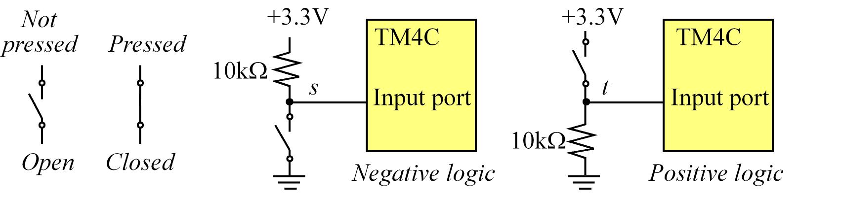
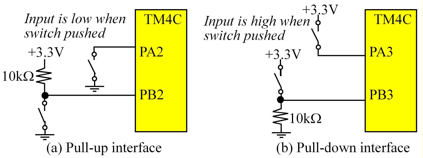
C8 Switches and LEDs
Switches
- We want to make sure that the pull-up or pull-down resistor is at least much bigger than the ON (close switch) resistor
of the switch but not as big as the OFF (open switch), usually 10kOhms will be good for most of the switches
- We also need take into consideration the Microcontroller Input Current
- e.g.
IiL = 2uA tells us that the current delivered by the uC is 2uA which means that if se use a 10kOhm the voltage would be V = R*I = (10k)*(2uA) = 0.2V which is fine since we have a range from 0V - 0.8V
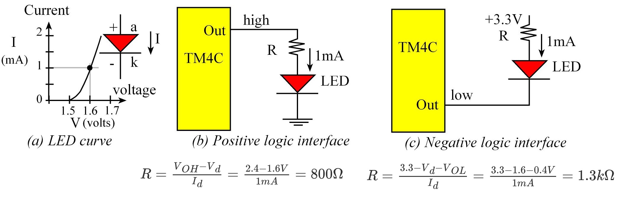
LEDs
- Anode (a
+): longer lead
- cathode (k
-): short lead (flat spot on the LED)
- Power in a LED is an indicator of brightness
- The most common implementation is to use negative logic so we must consider
VoL and the max current the uC can sink into a pin
C9 Arrays and Functional Debugging
Functional Debugging
Intrusiveness; let tmax be maximum time to execute the instrument, and let Δtmin be the minimum time in between calls
to the instrument (period of debugging call execution). The instrument is minimally intrusive if tmax/Δtmin is small (if this ratio is less than 1/1000)
Black-box testing is simply observing the inputs and outputs without looking inside. Black-box testing has an important place in
debugging a module for its functionality. On the other hand, white-box testing allows you to control and observe the internal workings of a system.
SysTick Timer
It is a 24-bit timer such that CURRENT counts down every bus cycle. After CURRENT counts to 0, it is automatically reloaded with the RELOAD value and continues to count.
It can used the System Clock; clock default = 16Mhz (without PLL) so decrements count every 62.5ns
Registers:
NVIC_ST_CTRL_R / CTRL: (ENABLE) Enables the Systick, (INTEN) it's interrupt, (CLK_SRC) the clock selection and also has the overflow flagNVIC_ST_RELOAD_R / RELOAD: 24-bits Reload valueNVIC_ST_CURRENT_R / CURRENT: 24-bits Actual count
Setup:
- Turn off
Systick by clearing ENABLE in the NVIC_ST_CTRL_R register
- Load value to
NVIC_ST_RELOAD_R
- Reset count by writing to
NVIC_ST_CURRENT_R register (In theory any value written should set it to 0)
- Write
0b101 to the NVIC_ST_CTRL_R register to enable counter, disable interrupts and select bus clock
The act of reading NVIC_ST_CTRL_R register when the COUNT flag is set will automatically clear it.
Also, writing any value to the NVIC_ST_CURRENT_R register will reset the counter to zero and clear the COUNT flag
#define NVIC_ST_CTRL_R      (*((volatile unsigned long *)0xE000E010))
#define NVIC_ST_RELOAD_R    (*((volatile unsigned long *)0xE000E014))
#define NVIC_ST_CURRENT_R   (*((volatile unsigned long *)0xE000E018))
#define SYSTICK_COUNT (0x00FFFFFF)

void SysTick_Init(void) {
  NVIC_ST_CTRL_R = 0;              // 1) disable SysTick during setup
  NVIC_ST_RELOAD_R = SYSTICK_COUNT;// 2) maximum reload value
  NVIC_ST_CURRENT_R = 0;           // 3) any write to current clears it
  NVIC_ST_CTRL_R = 0x00000005;     // 4) enable SysTick with core clock
}

unsigned long Now;      // 24-bit time at this call (12.5ns)
unsigned long Last;     // 24-bit time at previous call (12.5ns)
unsigned long Elapsed;  // 24-bit time between calls (12.5ns)
void Action(void){      // function under test
  Now = NVIC_ST_CURRENT_R;         // what time is it now?
  Elapsed = (Last-Now) & SYSTICK_COUNT; // 24-bit difference
  Last = Now;                      // set up for next...
}
Arrays & Strings
Arrays declared as global variables like other variables will be defined in RAM and we can place the data in ROM by using the const modifier, this data cannot be modified at run time..
The C compiler will add code that runs before your main, which will initialize all RAM-based variables to zero.
const actually means that the executing software cannot change the value at run time. This means in C programs not implemented on an embedded system, const data could be stored in RAM
In C, ASCII strings are just arrays pf characters stored with null-termination character at the end. In C, the compiler automatically adds the zero at the end, but in assembly, the zero must be explicitly defined.
It is good practice when dealing with strings is to specify the maximum reasonable string length. For example if we have a buffer of 100 bytes, the maximum string length will be 99 characters (1 byte reserved for \0 termination character)
C110 Finite State Machine
The Phase Lock Loop (PLL)
void PLL_Init(void) {
  // 0) Use RCC2
  SYSCTL_RCC2_R |=  0x80000000;  // USERCC2

  // 1) bypass PLL while initializing
  SYSCTL_RCC2_R |=  0x00000800;  // BYPASS2, PLL bypass

  // 2) select the crystal value and oscillator source
  SYSCTL_RCC_R = (SYSCTL_RCC_R & ~0x000007C0)   // clear XTAL field, bits 10-6
                               +  0x00000540;   // 10101, configure for 16 MHz crystal

  SYSCTL_RCC2_R &= ~0x00000070;  // configure for main oscillator source

  // 3) activate PLL by clearing PWRDN
  SYSCTL_RCC2_R &= ~0x00002000;

  // 4) set the desired system divider
  SYSCTL_RCC2_R |= 0x40000000;                   // use 400 MHz PLL
  SYSCTL_RCC2_R = (SYSCTL_RCC2_R & ~0x1FC00000)  // clear system clock divider
                  + (4 << 22);                   // configure for 80 MHz clock

  // 5) wait for the PLL to lock by polling PLLLRIS
  while((SYSCTL_RIS_R & 0x00000040) == 0);  // wait for PLLRIS bit

  // 6) enable use of PLL by clearing BYPASS
  SYSCTL_RCC2_R &= ~0x00000800;
}
Sync delay using SysTick
- Set the count base on:
tdelay = RELOAD_COUNT*(1/SysClk) and poll overflow flag
FSM: Finite State Machine
It's an abstraction used to describe a system that reacts to the inputs, changes states, and produces outputs
- In other words, it produces inputs based on some outputs and performs some logic that put the system in different states
A FSM can be described by 5 things:
- Set of inputs the system takes,
Input ∈ {In0, In1, ...}
- Set of outputs the system produces,
Output ∈ {Out0, Out1...}
- Set of states one can find the system,
CurrentState ∈ {S0, S1,...}
- The State Transition Graph (STG), which defines what causes the system to move from one state to another,
NextState = f(CurrentState , Input)
- Output determination (what determines the output), which tells us what is the corresponding output in each state,
Output = g(CurrentState)
Types of FSMs
- Moore FSM:
- The next state is dependent on the current state and the inputs
NextState = f(CurrentState , Input)
- The output depends on the current state
Output = g(CurrentState)
- There is a one-to-one correspondence between outputs and states so for each state, there is a unique output that's generated.
- Mealy FSM:
- The output depends on the current state and the input
Output = g(CurrentState, input)
A way to implement a FSM in C is using structures (struct)
Unlike an algorithm which gives a sequence of steps that need to be followed to realize the solution to a problem, a FSM describes the system (the solution being a realization of the system’s behavior) as a machine that changes states in reaction to inputs and produces appropriate outputs.
Motors
- Stepper motors are used in applications where precise positioning is more important than high RPM, high torque, or high efficiency.
UTAustinX: UT.6.20x Embedded Systems - Multi-Threaded Interfacing
C11 UART - The Serial Interface
General Communication Concepts
- There are three steps required for communication:
- Encode the information into packets (Talker thinks of the words to say)
- Transmission of the packets through a channel (Talker speaks and listener hears)
- The channel is the physical media through which the packets are sent.
- Decode the information (Listener interprets what the words mean)
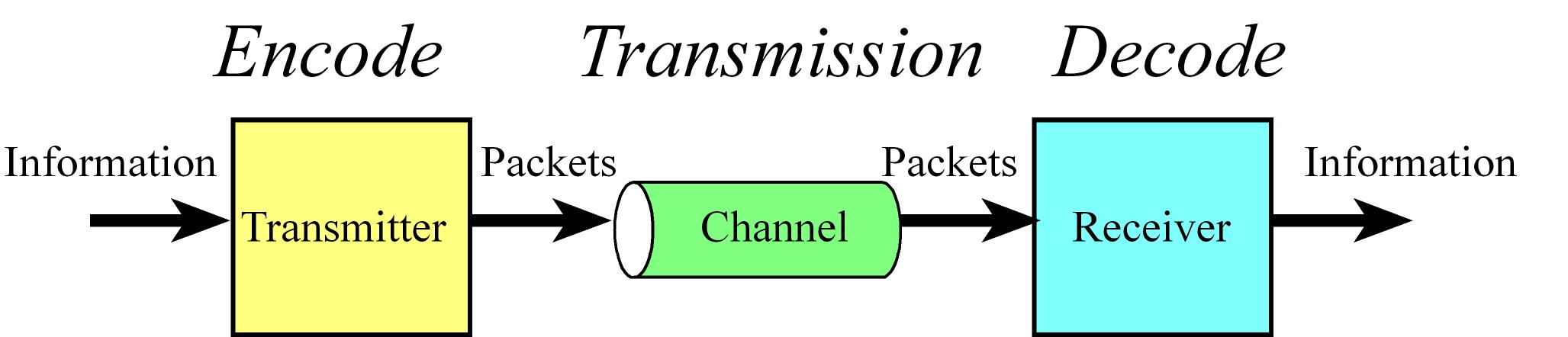
- Throughput or bandwidth is the maximum data flow in bytes/second that can be processed by the system.
- A performance measure is a quantitative metric that the goodness of the system.
- Full-duplex means transmission can occur in both directions simultaneously.
- Latency is the time between when the I/O device indicated service is required and the time when service is initiated.
- For an input device, software latency (or software response time) is the time between new input data ready and the software reading the data.
- For an output device, latency is the delay from output device idle and the software giving the device new data to output.
- For example in our data acquisition systems, we wish to invoke the analog to digital converter (ADC) at a fixed time interval. Software latency in this case is the time between when the ADC conversion is supposed to be started, and when it is actually started.
I/O Devices Synchronization
- Device Communication Requires Synchronization
- Synchronization is simply a process by which we bridge the speed mismatch between communicating devices.
- For how the software synchronizes with the hardware. There are usually the following mechanisms or a variant of these
to synchronize a processor/microcontroller with an I/O device:
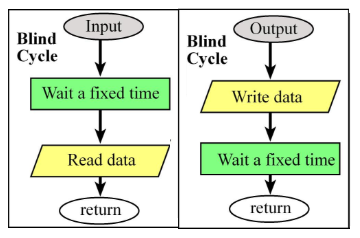
- Blind: Fixed delay in software,
- Software simply waits a fixed amount of time and assumes the I/O will complete before that fixed delay has elapsed.
- The delay or fixed amount of time to wait is determined based on the slowest device (e.g. in a uC using a UART, the slower I/O device in this case is the UART)
- For an input I/O device (to read) the software triggers (starts) the external input hardware, waits a specified time, then reads data from device.
- For an output I/O device (to write), the software writes data to the output device, triggers (starts) the device, then waits a specified time.
- Called blind, because there is no status information about the I/O device reported to the software. Used when the I/O speed is short and predictable
- E.g.: a LCD ASCII display we know we can wait 37us and then we are sure the operation is complete)
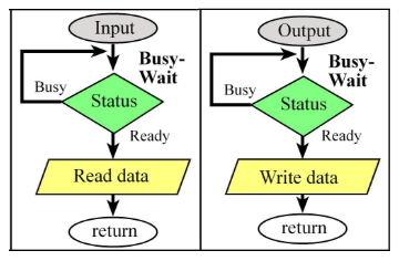
- Polling/Busy Wait: software checks a status flag in the device
- A Software loop checks the I/O status waiting for the done state or flag. A slight variation is Periodic polling in which software in a periodic interrupt checks a status flag
- For an input I/O device (to read) the software waits until the input device has new data, and then reads it from the input device
- For an output I/O device (to write), the software writes data, triggers the output device then waits until the device is finished
- Used in situations where the software system is relatively simple and real-time response is not important (E.g. UART to send/receive simple messages with no throughput requirements)
- Interrupt: Hardware triggers software when hardware is ready
- An interrupt uses hardware to cause special software execution.
- For an input I/O device (to read): the hardware will request an interrupt when input device has new data. The software interrupt service will read from the input device and save in global RAM or other shared data resource (queue, FIFO, list, etc.)
- For an output I/O device (to write): the hardware will request an interrupt when the output device is idle. The software interrupt service will get data from a global structure, and then write to the device.
- Used in situations where the system is fairly complex (e.g. a lot of I/O devices) or when real-time response is important.
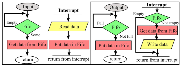
Direct memory access (DMA): sometimes is considered as a separate mechanism but in general it falls under the previous mechanisms since the hardware automatically transfers data and when hardware is ready signals with interrupt or sets flag(s) which are polled by SW. Used when high bandwidth and low latency are important
I/O bound, means the bandwidth is limited by the speed of the I/O hardware.
If the I/O device were faster than the software, then the software waiting time would be zero.
This situation is called CPU bound (meaning the bandwidth is limited by the speed of the executing software)
producer-consumer, bounded buffer and buffered I/O refers to the process of storing or buffering data in a first in first out (FIFO) queue
A Processor usually executes special software (called fault) when it tries to execute an illegal instruction, access an illegal memory location, or attempt an illegal I/O operation.
UART
TM4C123 has 8 UARTs but UART0 of is connected to the debugger which connects with USB to a PC and is used to emulate a COM port in the PC
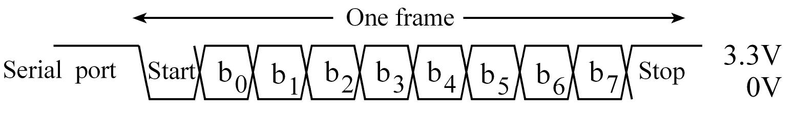
Idle is high
Frame has 10-bits: 1 start bit, 8-bits data and 1 stop bit
The number of bits per second is called Baud Rate ; BaudRate = 1/BitTime
UART Tx flow
- SW writes to Data register
- Data passes to Tx FIFO HW queue (16 elements buffer), use
TXFF which signals FIFO is full (1: full, 0: not full)
- Data is loaded into a 10-bits shift register for transmission
UART Rx flow
- HW receives data into a 10-bits shift register of Reception
- Once a dull frame is received is moved to Rx FIFO HW queue (16 elements buffer) which also store error bits for each frame:
- Frame Error -> BaudRate mismatch
- Overrun Error -> Rx FIFO buffer is full so data is lost
- There is also Parity Error and Break Error
- SW uses the RXFE flag = Rx FIFO empty == 1 that signal that there's no data to be consumed and when RXFE flag = Rx FIFO empty == 0 we know that there's at least some data
RXFE, is clear when new input data are in the receive FIFO. When the software reads from UART0_DR_R, data are removed from the FIFO
Even though the transmit data register is at the same address as the receive data register,
the transmit and receive data registers are two separate registers.
The transmission software can write to its data register if its TXFF (transmit FIFO full) flag is zero, which means there is space in the Tx FIFO.
The receiving software can read from its data register if its RXFE (receive FIFO empty) flag is zero, which means there is data in the Rx FIFO.
UART Config
- Turn on the UART clock in the
RCGC1 and Digital port clock in the RCGC2 register
- Enable pins as digital input, disable analog function, enable alt function and select UART Alt function
UARTX_CTL_R has bits to enable UART Tx (TXE) and Rx (RXE) and global enable (UARTEN) which must be cleared for init- Configure baud rate in
IBRD (integer ´part) and FBRD (fraction part = round(fraction*64) registers
Baud rate = Baud16/16 = (Bus clock frequency)/(16*divider)Actual Baud rate = (Bus clock frequency)/(16*(IBRD+(FBRD/64)))
UARTX_RSR_R has the UART errors and can be cleared by writing any value to it UARTX_FR_R has FIFOs status TXFF TXFE RXFF TXFE- The
BUSY flag in UARTX_FR_R is set while the transmitter still has unsent bits, even if the transmitter is disabled. It will become zero when the transmit FIFO is empty and the last stop bit has been sent.
- Out of reset, both FIFOs are disabled and act as 1-byte-deep holding registers. The FIFOs are enabled by setting the
FEN bit in LCRH.
  //------------UART_Init------------
  // Initialize the UART for 115,200 baud rate (assuming 80 MHz UART clock),
  // 8 bit word length, no parity bits, one stop bit, FIFOs enabled
  // Input: none
  // Output: none
  void UART_Init(void){
    SYSCTL_RCGC1_R |= SYSCTL_RCGC1_UART1; // activate UART1
    SYSCTL_RCGC2_R |= SYSCTL_RCGC2_GPIOC; // activate port C
    UART1_CTL_R &= ~UART_CTL_UARTEN;      // disable UART for init
    UART1_IBRD_R = 43;  // 80000000/(16*115200)) = 43.40278
    UART1_FBRD_R = 26;  //6-bbit fraction, round(0.40278 * 64) = 26
                                          // 8 bit word length (no parity bits, one stop bit, FIFOs)
    UART1_LCRH_R = (UART_LCRH_WLEN_8|UART_LCRH_FEN);
    UART1_CTL_R |= UART_CTL_UARTEN;       // enable UART
    GPIO_PORTC_AFSEL_R |= 0x30;           // enable alt funct on PC5-4
    GPIO_PORTC_DEN_R |= 0x30;             // enable digital I/O on PC5-4
                                          // configure PC5-4 as UART1
    GPIO_PORTC_PCTL_R = (GPIO_PORTC_PCTL_R&0xFF00FFFF)+0x00220000;
    GPIO_PORTC_AMSEL_R &= ~0x30;          // disable analog functionality on PC5-4
  }

  //------------UART_InChar------------
  // Wait for new serial port input
  // Input: none
  // Output: ASCII code for key typed
  unsigned char UART_InChar(void){
    while((UART1_FR_R&UART_FR_RXFE) != 0);
    return((unsigned char)(UART1_DR_R&0xFF));
  }

  //------------UART_OutChar------------
  // Output 8-bit to serial port
  // Input: letter is an 8-bit ASCII character to be transferred
  // Output: none
  void UART_OutChar(unsigned char data){
    while((UART1_FR_R&UART_FR_TXFF) != 0);
    UART1_DR_R = data;
    while((UART0_FR_R & UART_FR_BUSY) != 0); // Optional block until sent
  }

  // Iterative implementation
  // Number to ASCII
  void OutUDecIter(unsigned long n){
  unsigned cnt=0;
  char buffer[11];
    do{
      buffer[cnt] = n%10;// digit
      n = n/10;
      cnt++;
    }
    while(n);// repeat until n==0
    for(; cnt; cnt--){
      OutChar(buffer[cnt-1]+'0');
    }
  }

  // Recursive implementation
  // Number to ASCII
  void OutUDecRec(unsigned long n){
  if(n < 10){
    OutChar(n+0x30);  // base case
    return;
  }
  OutUDec(n/10);       // most significant digits
  OutChar(n%10+0x30);  // n%10 is 0-9
}
Networks and Distributed Systems
- A network is a collection of interfaces that share a physical medium and a data protocol.
- The topology of a network defines how the components are interconnected. E.g. rings, buses and multi-hop.
C12 Interrupts
An interrupt is the automatic transfer of software execution in response to a hardware event that is asynchronous with the current software execution.
A thread is defined as the path of action of software as it executes. Threads share access to I/O devices, system resources, and global variables, while processes have separate global variables and system resources.
Interrupts on the Cortex-M are controlled by the Nested Vectored Interrupt Controller (NVIC).
Requirements for Interrupt generation:
- Device Interrupt Enable a device to generate interrupts
- Global enable: On the ARM Cortex-M processor there is one interrupt enable bit for the entire interrupt system. In particular, to enable interrupts by writing a
0 to the I bit in PRIMASK.
- NVIC (Nested Vectored Interrupt Controller): Enable device interrupt in the interrupts module, for most devices there is an enable bit in the
NVIC that must be set.
- Level/Priority: The
BASEPRI register controls interrupts priority. E.g if the software sets the BASEPRI to 3, then requests with level 0, 1, and 2 can interrupt, while requests at levels 3 and higher will be postponed. If BASEPRI is zero, then the priority feature is disabled and all interrupts are allowed.
- Trigger: Refers to the actual HW async event that generates the interrupt. E.g. falling edge in an input
Context switch flow which happens when an interrupt occurs:
- The current instruction is finished
- The execution of the currently running program is suspended, pushing 8 registers on the stack (
R0, R1, R2, R3, R12, LR, PC, and PSR with the R0 on top). If the floating point unit is enabled an additional 18 words will be pushed
- The
LR is set to a specific value signifying an interrupt service routine (ISR) is being run (to signify this, LR bits [31:8] are set to 0xFFFFFF, and bits [7:0] specify the type of interrupt return to perform)
- The
IPSR is set to the interrupt number being processed
PC is loaded with the address of the ISR- ISR code starts executing

Context switch, occur automatically in hardware as the context is switched and we can also have a context switch from a lower
priority ISR to a higher priority ISR
When one interrupt preempts another, the LR is set to 0xFFFFFFF1
If a trigger flag is set, but the interrupts are disabled (I=1), the interrupt level is not high enough,
or the flag is not enabled to generate interrupt, the request is held pending so under most cases it remains set until the software clears it.
An atomic operation is a sequence that once started will always finish and cannot be interrupted.
To return from an interrupt, the ISR executes the typical function return statement: BX LR. However, since the top 24 bits of LR are 0xFFFFFF, it knows to return from interrupt by popping the eight registers off the stack.

Interrupt Service Routine (ISR)
The interrupt service routine (ISR) is the software module that is executed when the hardware requests an interrupt.
Usually there are many small ISRs specific for each potential source of interrupt (vectored interrupts).
In most cases the ISR is where the software must explicitly clear the trigger flag that caused the interrupt (acknowledge).
After the ISR provides the necessary service, it will execute a return instruction (E.g. BX LR) and because LR contains a special value his instruction pops the appropriate registers from the stack (8 if float-point is disabled or 26 if it is), which returns control to the main program
An axiom with interrupt synchronization is that the ISR should execute as fast as possible
If the average time to run ISRi is ΔTi and the average time between executions of this ISR is δTi, then the average utilization
of this interrupt is Ui = ΔTi /δTi because of this the minimum δTi must be greater than the maximum ΔTi, it order to guarantee no interrupts are lost
and the total utilization U = sum(Ui) = sum(ΔTi /δTi) for i = 0 to TOTAL_INTERRUPTS-1 must be < 1
The utilization formulas are saying NOT to have the interrupt service routine take longer than the time between interrupts, so the time between the interrupts. This should be long compared to the time it takes to execute the interrupt service routine.
Inter-Thread Communication and Synchronization
For regular function calls, we use the registers and stack to pass parameters, but interrupt threads have logically
separate registers and stack. More specifically, registers are automatically saved by the processor as it switches
from the main program to the interrupt service routine
In order to pass information between the main program and the ISRs we need Communication and Synchronization
one way to do this is using constructs to synchronize threads like:
- A binary semaphore is simply a shared flag, we can Signal the semaphore which sets the flag or Wait for it which is the action that checks the flag
- A mailbox is like a 1 element FIFO with field: data which contains actual data and status to signal if there's data
- A FIFO is an order preserving construct that contains data elements and a status to signal if there is data, we
put data to add elements and get to extract data
Interrupts on the ARM Cortex-M Processor
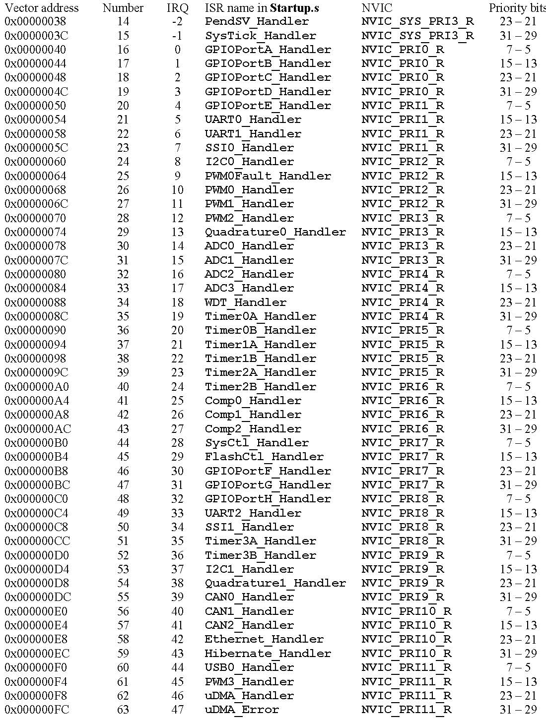
Each Interrupt has an associated 32-bit vector that points to the memory location where the ISR that handles the interrupt is located.
Vectors are stored in ROM at the beginning of memory.
Location 0x00000004 There are up to 240 possible interrupt sources and their 32-bit vectors are listed in order starting with location 0x0000.0008. contains the initial program counter, which is also called the reset vector. It points to a function called the reset handler,
which is the first thing executed following reset. In C, the reset handler initializes global variables and then calls your main() program
There are up to 240 possible interrupt sources and their 32-bit vectors are listed in order starting with location 0x00000008
Vectors are in ROM, so this linkage is defined at compile time and not at run time.
Each NVIC Priority register (NVIC_PRIx_R) contains an 8-bit priority field for four devices. On the TM4C microcontrollers, only the top three bits of the 8-bit field are used. This allows us to specify the interrupt priority level for each device from 0 to 7, with 0 being the highest priority
To enable a device interrupt on the NVIC side we must use set bits on the NVIC_ENx_R and to disable we must also set bits but on the NVIC_DISx_R
SysTick is the only interrupt on the TM4C that has an automatic acknowledge. So technically we don't need to clear any flag
GPIO Interrupts Config:
- Config pin for general digital input -> GPIO Config
- Select level or edge triggering type in
IS, IEV and IBE registers
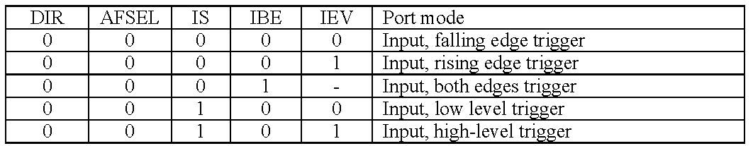
- Setup
IME bits to enable interrupt in the port pin. Also is a good practice to clear the interrupt flag before enabling the interrupt
- Enable interrupt in the
NVIC and make sure global interrupts are enabled (optionally set priority)


- On interrupt for the port check which bit generate the interrupt using the flag in the
GPIO_PORTx_RIS_R register
and clear it by writing to the GPIO_PORTx_ICR_R corresponding bit
  volatile unsigned long SW1, SW2;
  void EdgeCounter_Init(void){
    SYSCTL_RCGC2_R |= 0x00000020;     // (1) activate clock for port F
    SW1 = SW2 = 0;                    // (1) initialize counters and wait for clock
    GPIO_PORTF_LOCK_R = 0x4C4F434B;   // (1) unlock GPIO Port F
    GPIO_PORTF_CR_R = 0x1F;           // (1) allow changes to PF4,PF0
    GPIO_PORTF_DIR_R &= ~0x13;        // (1) make PF4,PF0 in (built-in button)
    GPIO_PORTF_DEN_R |= 0x13;         //     enable digital I/O on PF4,PF0
    GPIO_PORTF_PUR_R |= 0x11;         //     enable weak pull-up on PF4,PF0

    GPIO_PORTF_AFSEL_R &= ~0x13;      //     disable alt funct on PF4,PF0
    GPIO_PORTF_PCTL_R &= ~0x000F000F; //     configure PF4,PF0 as GPIO
    GPIO_PORTF_AMSEL_R &= ~0x13;      //     disable analog functionality on PF4,PF0

    GPIO_PORTF_IS_R &= ~0x11;         // (2) PF4,PF0 is edge-sensitive
    GPIO_PORTF_IBE_R &= ~0x11;        //     PF4,PF0 are not both edges
    GPIO_PORTF_IEV_R &= ~0x11;        //     PF4,PF0 falling edge event
    GPIO_PORTF_ICR_R = 0x11;          // (x) clear flags

    GPIO_PORTF_IM_R |= 0x11;          // (3) arm interrupt on PF4,PF0

    NVIC_PRI7_R = (NVIC_PRI7_R & 0xFF00FFFF) | 0x00A00000; // (4) priority 5
    NVIC_EN0_R = 0x40000000;                               // (4) enable interrupt 30 in NVIC
    EnableInterrupts();                                    // (4) Enable global Interrupt flag (I)
  }

  void GPIOPortF_Handler(void ){
    if(GPIO_PORTF_RIS_R & 0x10) { // poll PF4
      GPIO_PORTF_ICR_R = 0x10;    // acknowledge flag4
      SW1++;                      // signal SW1 occurred
    }

    if(GPIO_PORTF_RIS_R & 0x01) { // poll PF0
      GPIO_PORTF_ICR_R = 0x01;    // acknowledge flag0
      SW2++;                      // signal SW2 occurred
    }
  }

  int main(void){
     EdgeCounter_Init(); // initialize GPIO Port F interrupt
     while(1){
        WaitForInterrupt();
     }
  }
C13 DAC and Sound
Digitization
- An analog signal is one that is continuous in both amplitude and time e.g., voltage, current, position, angle, speed, force, pressure, temperature, etc.
- To represent a signal in the digital domain we must approximate it in two ways: amplitude quantizing and time quantizing (or Sampling)
- To quantize we need to place limits on the signal restricting it to exist between a minimum and maximum value and divide this amplitude range into a finite set of discrete values. The range of the system is the maximum minus the minimum value
- The precision of the system defines the the number of levels we can represent in a signal (the number of alternatives), usually given in bits 8-bits => 256 different values
- The resolution is the smallest change in value I can represent in the analog signal (The smallest change that is significant).
- Time quantizing is caused by periodic capture of samples (Sampling) which restricts the signal to a finite time
Nyquist Theorem
- The Nyquist Theorem states that
- if the signal is sampled with a frequency of
fs, then the digital samples only contain frequency components from 0 to ½ fs.
- if the analog signal does contain frequency components larger than
½ fs, then there will be an aliasing error during the sampling process (performed with a frequency of fs).
- Aliasing is when the digital signal appears to have a different frequency than the original analog signal.
- The frequency of a signal (
f) to be sampled must be less than half of the sampling frequency f < ½ fs => fs > 2*f => Ps > P/2 to avoid Aliasing
DAC
Sound as an Analog Signal
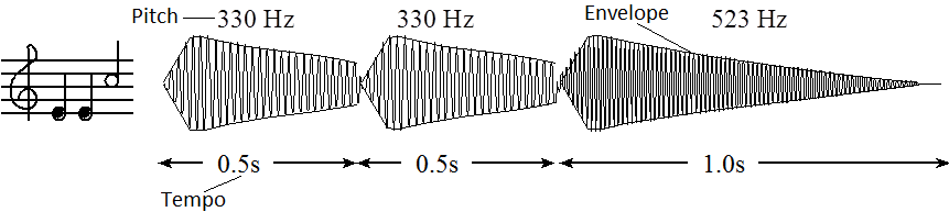
- Loudness of the tone is determined by the amplitude of the wave
- The pitch (Spanish: tono) is defined as the frequency of the wave.
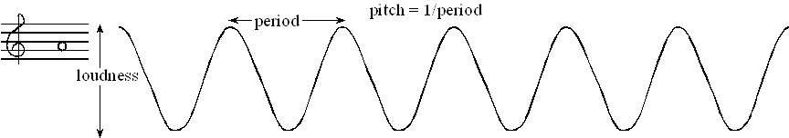
- The tempo of the music defines the speed of the song A moderate tempo a quarter note has a duration of
½ second
- The envelope of the note defines the amplitude versus time relationship
- A chord is created by playing multiple notes simultaneously, the sounds are mixed arithmetically. You can create the same effect by adding two waves together in software
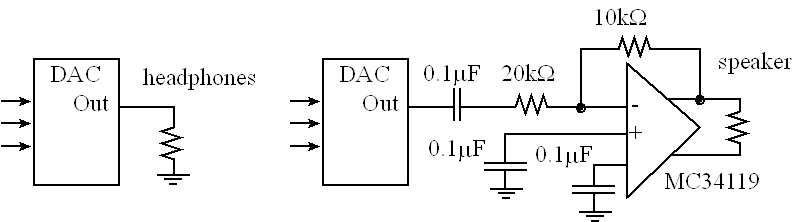
MC34119 can be used to create a simple audio amplifier
C14 ADC and Data Acquisition
- A sensor or transducer/transductor is used to convert a physical parameter into an electrical parameter.
- The ADC range is the maximum and minimum ADC input (e.g. 0 to +3.3V) and it's resolution is the smallest distinguishable change in input (e.g. 3.3V/4096 = ~0.81 mV).
Range(volts) = Precision(alternatives) * Resolution(volts)
- Most ADCs are implemented using successive approximation and usually it's conversion speed is linear with the number of bits.
- The Speed of the ADC (How fast we can sample) involves both the ADC conversion time (how long it takes to convert), and the bandwidth (what frequency components can be recognized by the ADC).
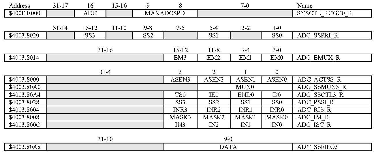
ADC Config
- Pin Config Enable the port clock for the pin that we will be using for the ADC input, make the pin an input with
DIR, enable alt function (AFSEL), disable digital function (DEN), activate the analog interface in the pin with AMSEL
- Specify sample rate in
SYSCTL_RCGC0_R and enable the ADC clock
- Disable the sequencer in the
ADC0_ACTSS_R during setup, select it's priority in ADC0_SSPRI_R, usually we just need one sequencer so priorities are irrelevant but no two sequencers should have the same priority,
- Use
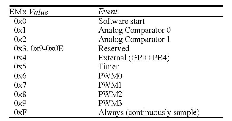
EM3 in the ADC0_EMUX_R register to specify how the ADC will be triggered. For software trigger (EM3 = 0) the software
writes an 8 (set SS3) to the ADC0_PSSI_R to initiate a conversion on sequencer 3.
Select ADC channel input source, ADC0_SSMUXn_R defines which channel is sampled, also clear SS3 for good practice. There are twelve ADC channels on the LM4F120/TM4C123.
Configure the sample control, the ADC0_SSCTL3_R register specifies the mode of the ADC sample.
- Set
TS0 to measure temperature and clear it to measure the analog voltage
- Set
IE0 so that the INR3 bit is set when the ADC conversion is complete, to clear INR3 we must write to the corresponding bit in ADC0_ISC_R register
END0 signify sample is the end of the sequenceD0 bit activates differential sampling use to measure the analog difference between two ADC pins, usually disabled
When programming the last nibble, ensure that the END bit is set.
Enable the sequencer in the ADC0_ACTSS_R using the ASENn bit
The most accurate sampling method is timer-triggered sampling (EM3 = 0x5)
void ADC0_InitSWTriggerSeq3_Ch9(void){
  volatile unsigned long delay;

  SYSCTL_RCGC2_R |= 0x00000010;   // 1) activate clock for Port E
  delay = SYSCTL_RCGC2_R;         //    allow time for clock to stabilize
  GPIO_PORTE_DIR_R &= ~0x04;      // 1) make PE2 input
  GPIO_PORTE_AFSEL_R |= 0x04;     // 1) enable alternate function on PE2
  GPIO_PORTE_DEN_R &= ~0x04;      // 1) disable digital I/O on PE2
  GPIO_PORTE_AMSEL_R |= 0x04;     // 1) enable analog function on PE2

  SYSCTL_RCGC0_R |= 0x00010000;   // 2) activate ADC0 clk
  delay = SYSCTL_RCGC2_R;
  SYSCTL_RCGC0_R &= ~0x00000300;  // 2) configure for 125 KSamples/s

  ADC0_SSPRI_R = 0x0123;          // 3) Sequencer 3 = 0 so is the one with highest priority
  ADC0_ACTSS_R &= ~0x0008;        // 3) disable sample sequencer 3 for setup

  ADC0_EMUX_R &= ~0xF000;         // 4) seq3 is software trigger

  ADC0_SSMUX3_R &= ~0x000F;       // 5) clear SS3 field
  ADC0_SSMUX3_R |= 0x01;          //    set channel Ain1 (PE2)
  //ADC0_SAC_R = 0x06;            // Optional set Hardware Averaging Control (Oversampling)
  ADC0_SSCTL3_R = 0x0006;         // 6) no TS0 D0, yes IE0 and END0
  ADC0_ACTSS_R |= 0x0008;         // 7) enable sample sequencer 3

}

//------------ADC_InSeq3------------
// Polling (Busy-wait) analog to digital conversion
// Input: none
// Output: 12-bit result of ADC conversion
unsigned long ADC0_InSeq3(void){
  unsigned long result;
  ADC0_PSSI_R = 0x0008;               // 1) initiate SS3
  while((ADC0_RIS_R & 0x08) == 0){};  // 2) wait for conversion done
  result = (ADC0_SSFIFO3_R & 0xFFF);  // 3) read result
  ADC0_ISC_R = 0x0008;                // 4) acknowledge completion, clear flag

  return result;
}
C15 Systems Approach to Game Design
A software module is a self-contained software task with clear entry and exit points.
A module is usually a collection of functions that in its entirety performs a well-defined set of tasks
A device driver is a software module that facilitates the use of I/O, it is a collection of software functions for a particular I/O device
Information hiding is similar to minimizing coupling. It is better to separate the mechanisms of software from its policies.
We should separate “what the function does” from “how the function works”
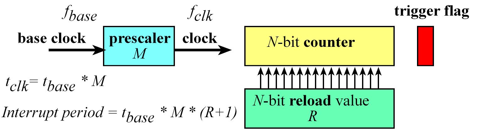
Timer
The TM4C123 has six timer modules 0 to 5 and each module is divided into two 16-bit timers (TimerA and TimerB) that can be combined to create 32-bit timers
When the timer counts from 1 to 0 it sets the trigger flag so every time it hits the 0 value the trigger flag becomes a 1
TIMERn_TAILR_R has the reload value, and periodic timer mode is the most common usage in which the timer runs continuously
The Period of the timer will be P = tbase*M*(R + 1) so => R = (P /(tbase*M )) – 1
R: Reload value
tbase be the period of the base clock (for 80MHz => 12.5ns).
M will be a pre-scaler, which sits between the base clock and the clock used to decrement the counter. M is greater than or equal to 1 and can be configured to slow down the counting
Timer config
- Enable clock to timer by setting bit 2 in
SYSCTL_RCGCTIMER_R
- Disable timer for setup in
TIMER2_CTL_R
- Configure n-bits mode in
TIMER2_CFG_R
- Configure timer mode in
TIMER2_TAMR_R
- Setup reload value in
TIMER2_TAILR_R
- Setup clock resolution in
TIMER2_TAPR_R
- Write 1 to clear interrupt flag in
TIMER2_ICR_R
- Enable interrupts for timer setting
TATOIM bit in TIMER2_IMR_R
- Setup interrupt priority in
NVIC_PRIx_R register
- Enable interrupt in
NVIC in corresponding NVIC_ENx_R registers
- Enable Timer after setup is completed in
TIMER2_CTL_R
unsigned long TimerCount;
void Timer2_Init(unsigned long period) {
  unsigned long volatile delay;
  SYSCTL_RCGCTIMER_R |= 0x04;   // 0) activate clock to timer2 (you can also use SYSCTL_RCGC1_R legacy register)
  delay = SYSCTL_RCGCTIMER_R;
  TimerCount = 0;
  TIMER2_CTL_R = 0x00000000;                             // 1) disable timer2A (set to 0 to disable, 1 to enable)
  TIMER2_CFG_R = 0x00000000;                             // 2) 32-bit mode (set to 0 for 32-bit mode)
  TIMER2_TAMR_R = 0x00000002;                            // 3) periodic mode (set to 2 for periodic mode)
  TIMER2_TAILR_R = period-1;                             // 4) reload value
  TIMER2_TAPR_R = 0;                                     // 5) clock resolution (set to 0 for 12.5ns)
  TIMER2_ICR_R = 0x00000001;                             // 6) clear timeout flag (write 1 to bit 0)
  TIMER2_IMR_R = 0x00000001;                             // 7) arm timeout (TATOIM is bit 0)
  NVIC_PRI5_R = (NVIC_PRI5_R & 0x00FFFFFF) | 0x80000000; // 8) Set interrupt priority to 4
  NVIC_EN0_R |= 1<<23;                                    // 9) enable IRQ 23 => timer2A interrupt
  TIMER2_CTL_R = 0x00000001;                             // 10) enable timer2A
}

// trigger is Timer2A Time-Out Interrupt
// set periodically TATORIS set on rollover
void Timer2A_Handler(void) {
  TIMER2_ICR_R = 0x00000001;  // acknowledge
  TimerCount++;
// run some background stuff here
}

void Timer2A_Stop(void) {
  TIMER2_CTL_R &= ~0x00000001; // disable
}

void Timer2A_Start(void) {
  TIMER2_CTL_R |= 0x00000001;   // enable
}
C16 Internet of Things
point-to-point communication means there's only two endpoints and they talk to each.
In Carrier Sense Multiple Access Collision Detection (CSMA/CD) protocol a node puts a communication request onto the medium and hope that nobody else is communicating.
If nobody else is communicating, then the communication is going to go through. If somebody else also senses it to be idle and they try to communicate, then there will be a collision.
Ethernet protocol (IEEE 802.3) uses CSMA/CD
The wireless standards (like WiFi IEEE 802.11 and the Bluetooth IEEE 802.15 protocols) use variations of the CSMMA/CD called Carrier Sense Multiple Access-Collision Avoidance (CSMA/CA) in which carrier sensing is used and besides nodes attempt to avoid collisions by transmitting only when the channel is sensed
Internet Summary
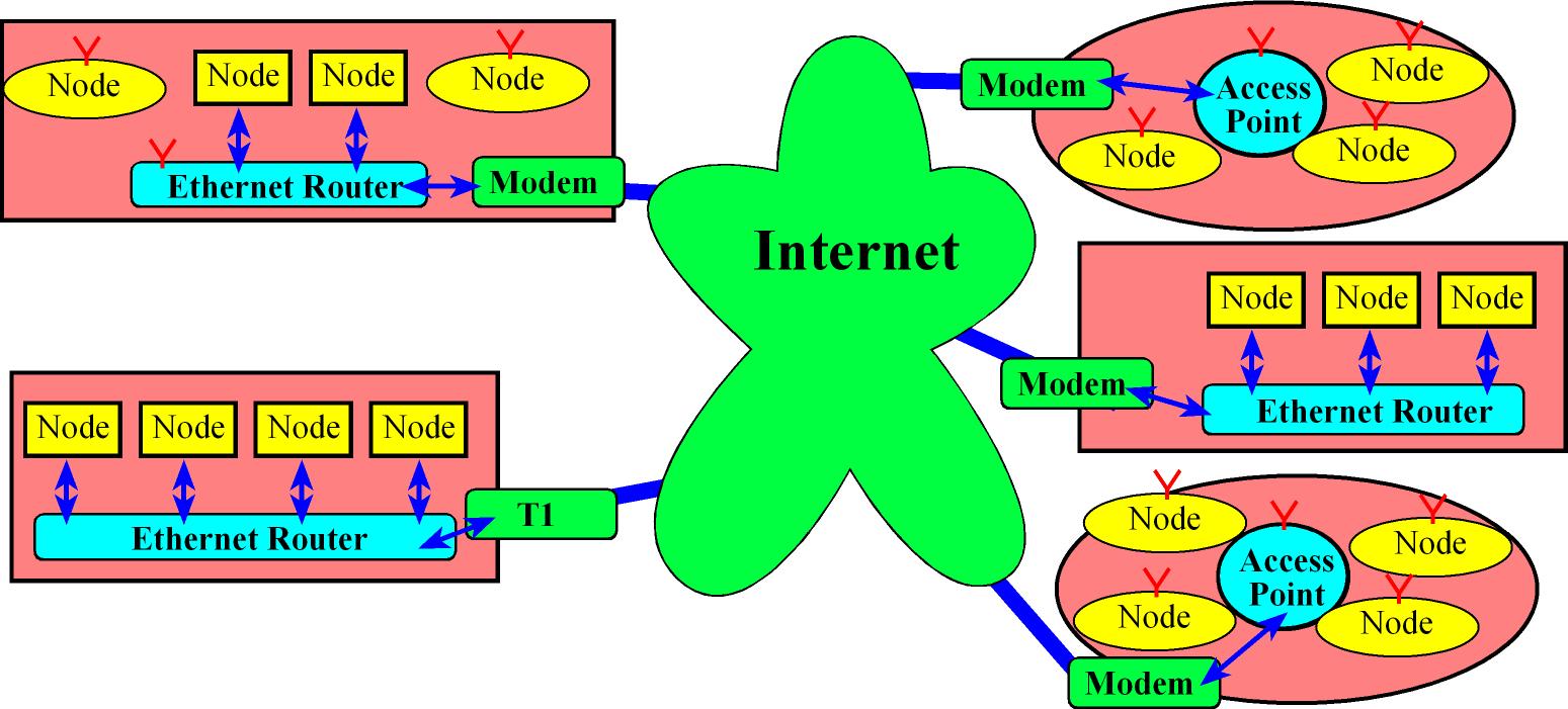
Once we configure machines to communicate with each to other as a small local area network (LAN), the next logical challenge is to make multiple such LANs to communicate with each other. This interconnection of networks is the Internet,
The collective issues concerning the interconnection of networks are addressed by what is called the Network layer. It handles:
- Addressing Assignment of IP addresses to identify devices. A lookup service called Domain Name Service (DNS), is also needed to map symbolic names to its corresponding IP address
- Routing the movement of information (packaged in chunks called Datagrams) from one machine to another in an optimal way, this routing problem is solved by using the Internet Group Management Protocol (IGMP) which is basically an optimal routing algorithm.
The Address Resolution Protocol (ARP) protocol’s target is to get every machine to learn the hardware address and the corresponding IP address of every other machine in a LAN.
Each machine has multiple ports at which it can send and receive messages.
The Transport layer is responsible for providing this abstraction of ports and implementation.
- TCP ports: reliable communication
- UDP ports: unreliable best-effort communication.
- Ports are software constructs that explicitly are just 16-bit numbers so a device can have up to
2^16=65536 different ports
An end-point of communication can be seen as containing, a port number, its type (TCP/UDP) and the IP address.
it's an abstraction that contains all the information to establish a communication between applications running in different devices.
A socket captures this end-point from a programmer’s perspective, therefore programming in the Internet is nothing but using the socket API
A socket is an application endpoint for communication that encapsulates IP address, the transport protocol and the port.
Higher level Application layer protocols use sockets for their implementation
- E.g. HTTP, SMTP, FTP use sockets that are TCP-based for reliability and Multimedia applications like VoIP use UDP sockets as the goal there is speed and not reliability
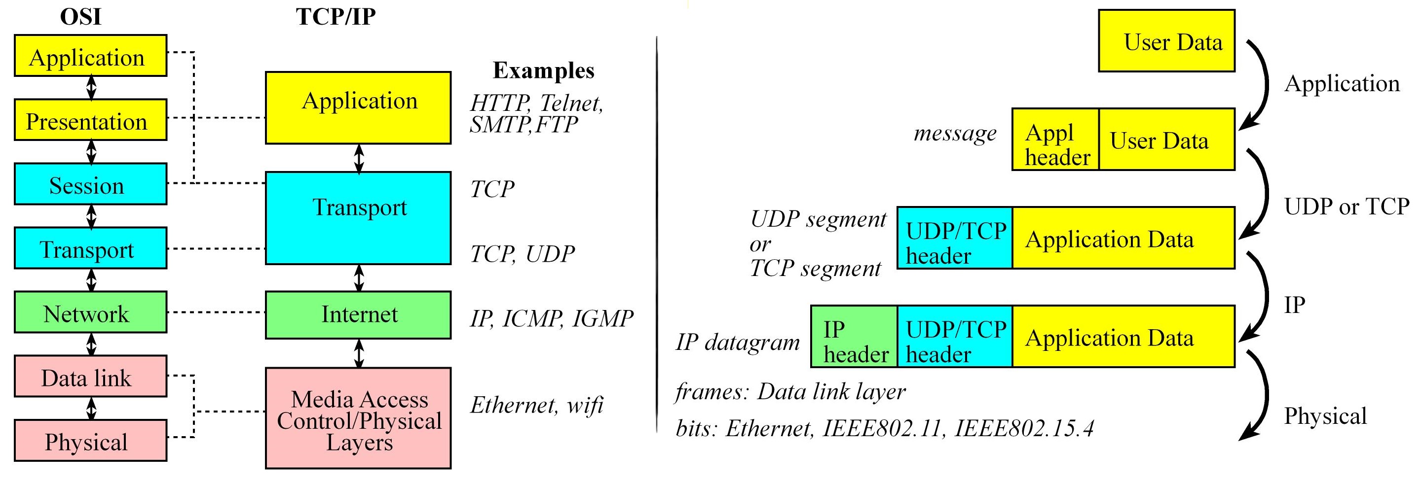
Internet Layered model:
- Application layer
- Adds Application header which is specific to the application -> Message
- Transport layer
- Adds TCP/UDP Header with port information and checksum for integrity -> TCP/UDP Packet/Segment
- Network layer
- Adds IP Address and routing information -> IP Datagram
- Media Access Layer.
- Adds specific media access header -> Frame
IP
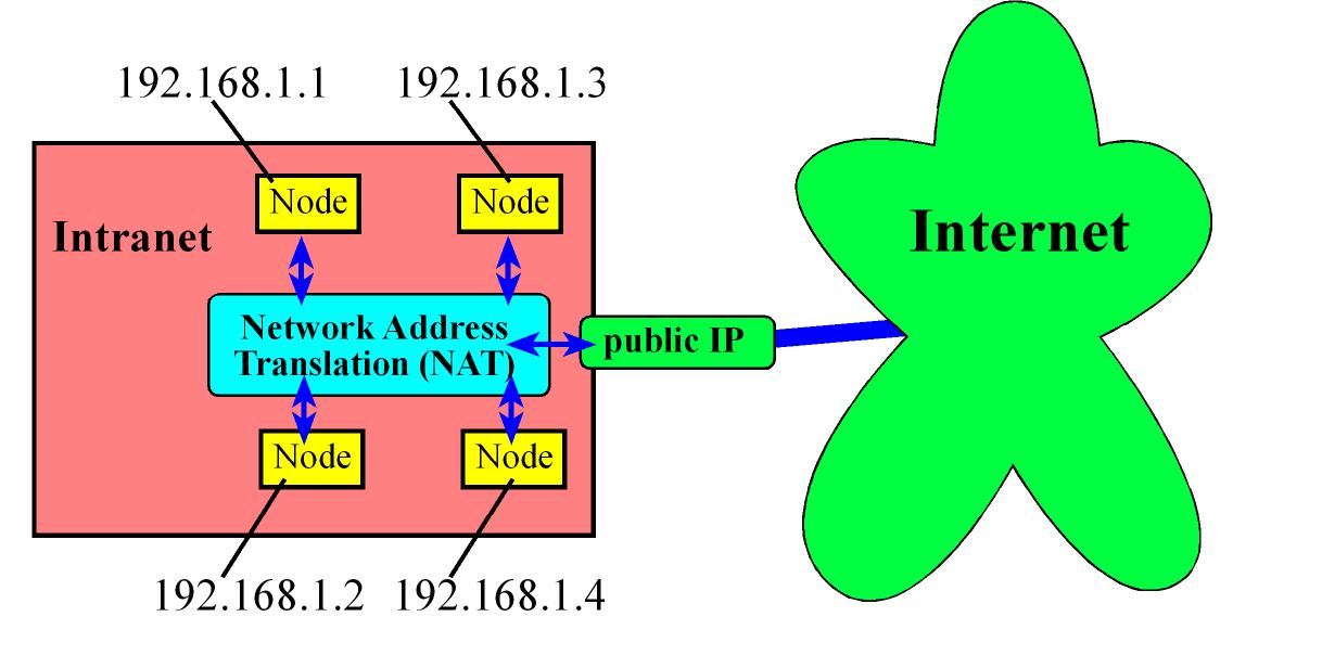
With 32-bit IP Addresses inevitable we will run out of unique IP addresses to solve this the IETF set aside IP addresses that can be used in private networks.
- These private IP addresses could be used for embedded devices within Intranets
By using a technique called Network Address Translation (NAT) these embedded devices inside Intranets can communicate (if needed) with other entities in the Internet, by sharing one non-private IP address among a set of devices.
An Intranet is a local network than communicates with each other using private IP addresses. The Network Address Translation (NAT) routes incoming messages to the public IP address to the correct private address.
| Start |
End |
Number of addresses |
| 10.0.0.0 |
10.255.255.255 |
2^24 |
| 172.16.0.0 |
172.31.255.255 |
2^20 |
| 192.168.0.0 |
192.168.255.255 |
2^16 |
If we remove the amount of private addresses we have 2^32 - 2^24 - 2^20 - 2^16 = 4294967296 - 17891328 = 4,277,075,968 which is still about 2^32 addresses.
IoT: Internet of things
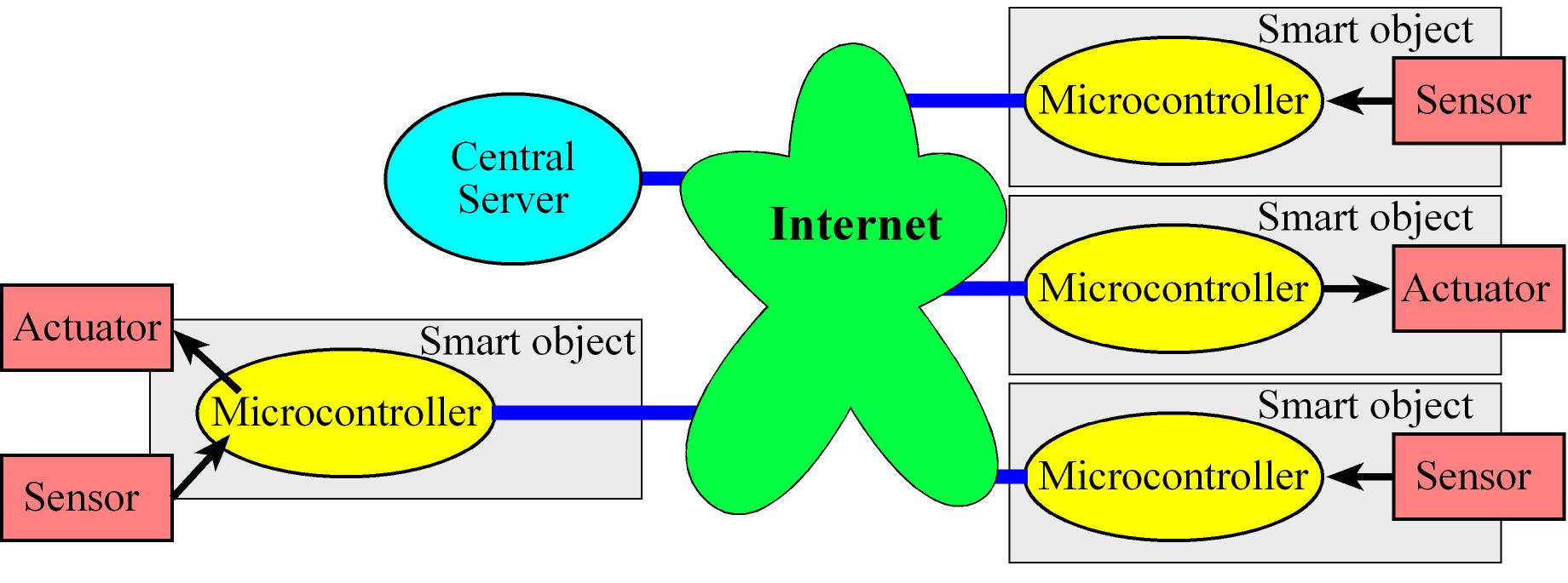
The Internet of things (IoT) is the combination of embedded systems, which have sensors to collect data and actuators to affect the surrounding, and the internet, which provides for ubiquitous remote and secure communication.
- A thing is an embedded system with inputs and outputs performing a dedicated function.
A distributed solution deploys multiple sensors and actuators connected by the internet
uIP is a light-weight implementation of the IP stack
- Security in IoT:
- Confidentiality: We must decide what it means to view/change the data and who has the right to read/write. For this we need:
- Authentication which is the means to ensure the identity of the sender is correct.
- Encryption which makes it harder for an unauthorized party to view a message
- Data integrity: It is important that data reach the rightful recipient in an unaltered fashion, for this we need techniques that support both detection and prevention
- Availability: A secure communication not only requires the correct data arrive at the correct place, but also at the correct time (E.g. DDoS resistant)
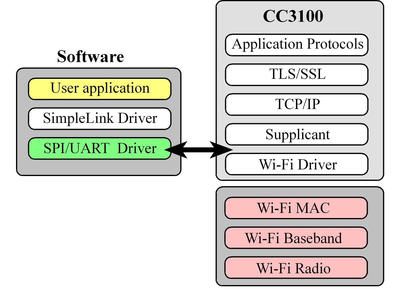
WiFi Interface: CC3100 Booster Pack
The CC3100 is the hardware support (physical hardware and firmware) to communicate using WiFi, this device shifts most of the
internet layers onto firmware and a small Software footprint remains on the host microcontroller
- Texas Instruments calls this footprint SimpleLink.
The CC3100 could be interfaced with either SSI2 (PB4-7, PE0) or UART1 (PB0, PB1, PC4, PC5).
The actual TCP/IP software stack resides in firmware on the CC3100 booster pack itself, that's why is recommended to upgrade the FW
CC3200 (which is a never version of the CC3100) is a device containing both the internet stack and a general purpose microcontroller on a single chip.
Client-Server
References